Lines of activity
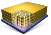
Three-dimensional integrated microsystems
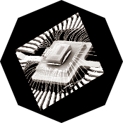
In recent years miniaturization of microelectronic products goes along with improving of their functionality through the integration of formed micro mechanical, optical and biological systems, improving of their characteristics, decrease of consumed energy, increase of productivity and cost reduction. The possible way of resolving all these problems is 3D-assembling. It allows to create compact micro assembling of polytypic microelectronic products (microprocessors, core storage, variety of sensors, etc.). This significantly reduces a number of switching in manufacturing of final products that is leading to substantial decrease of losses and increasing of products reliability.
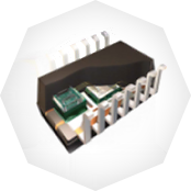
Thus 3D-integration gives the following advantages:
- High degree of integration;
- Decreasing of interconnection lines length;
- Increasing of signal rate;
- Decreasing of consumed energy;
- Integration of different technologies.
Technology of 3D-assembling provides several methods of integration:
 Integration chip-on-wafer
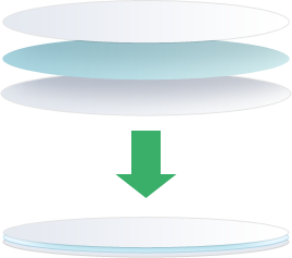 Integration wafer-on-wafer or vertical system of integration (VSI)
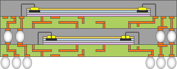 Integration package-on-package
Chip stacking assembly with chips boiled soft (for creation of interconnections) is designing by such companies as Intel, Hitachi, Amkor, Philips, etc. during several years already. Even more advantages gives assembling of chips on each other on the level of wafer. It promotes increasing of productivity and cost reduction.
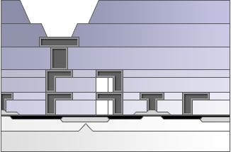
Vertical system of integration (VSI) is characterized by creation of high density outlets between chips. These outlets are formed by means of creation through via in silicon that's why this technology is called TSV (Trough Silicon Via). TSV technology is based on processes of thinning, assembling and vertical metallization of completely finished silicon wafer with microschemes.
Vertical system of integration based on TSV technology gives a number of advantages:
- Provides higher density of assembling at the same sizes;
- Allows to achieve higher functionality;
- Substantially decreases the interconnection lines length and increases the signal rate;
- Helps to decrease energy consumption and reduce cost of the final product.
3D-assembling based on TSV technology includes the following stages:
- Creation of via (laser threading, deep reactive ion etching);
- Filling of via with metal (usually using copper);
- Assembling of wafers on each other (combination and assembling);
- Thinning of wafers before chips assembling (smoothing, chemical etch).
 Assembling of chips on wafer and wafer on wafer.